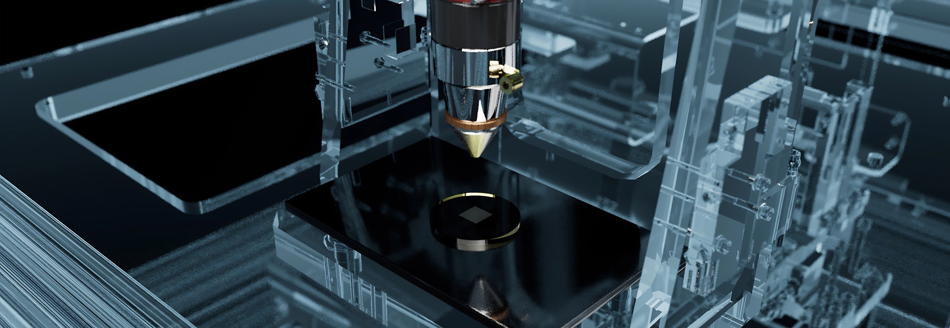
Micro-Nano Photonics Technology
This technology involves the design, fabrication, and application of optical components with features at the micron or nanometer scale
Liquid Crystal Micro-Nano Photonics
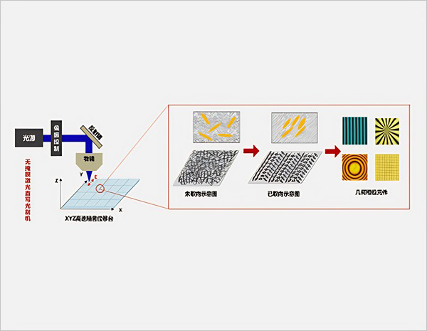
By using maskless laser direct writing technology, two-dimensional geometric phase optical elements with micro- and nanometer-scale features are fabricated on the substrate surface through light-controlled alignment. This includes self-developed core materials, essential equipment, and a complete process flow, establishing the first mass production line in China based on liquid crystal micro-nano photonics technology.
Etching Process
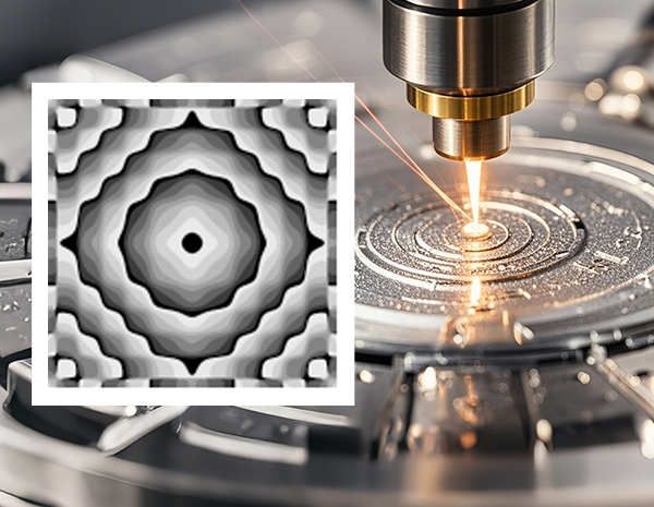
Phase structures are designed with computer-aided design (CAD) and simulated for etching tolerance analysis. Using semiconductor techniques, material is etched away from the substrate surface to enhance the damage threshold of the component. The etched diffractive optical elements (DOE) are characterized in combination with application-specific optical path design.
Ultrafast Laser Processing
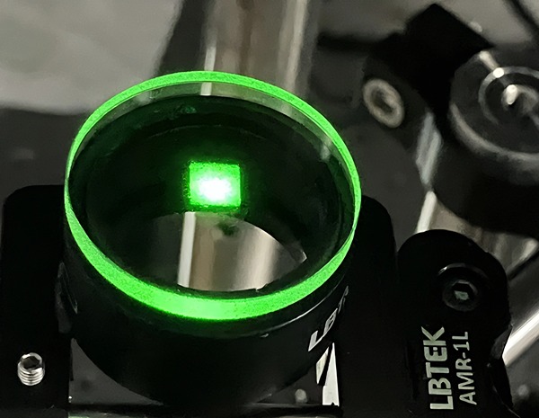
Ultrafast laser modifies the internal structure of quartz to induce birefringence. This allows the orientation of the modified region to vary within a two-dimensional plane, enabling geometric phase modulation.
 Wechat
 Tiktok
 Zhihu
Zhihu
 Bilibili